The power management IC (PMIC) passed every electrical test and had a maximum junction temperature of 125°C. The thermal budget allowed a 40°C rise from the 25°C ambient condition, giving an apparently comfortable margin. Yet the product experienced a 23% field failure rate after 18 months, far short of its 10-year reliability target. Failure analysis identified electromigration damage in the PMIC’s metal interconnects.
The problem was not the datasheet value itself, but the thermal assumptions used in the design. The analysis used the PMIC’s junction-to-case thermal resistance and a generic board-level convection coefficient, but did not account for the 6 W DSP located just 8 mm away on a 4-layer FR4 board with minimal copper pour. Heat from the DSP raised the PMIC’s local ambient temperature by 28°C, increasing its junction temperature from the estimated 65°C to 93°C under full load. Because electromigration is highly temperature-dependent, this temperature increase made the electromigration rate 11 times higher than assumed.
This is the failure mode of inadequate thermal simulation: the calculation may be correct, but the model can still be too simple for the physical situation. A one-dimensional thermal resistance network cannot capture heat transfer between adjacent components, non-uniform PCB temperatures, actual enclosure airflow, or transient temperature changes during power cycling. Each effect can shift junction temperature by 10–30°C, potentially increasing the rate of thermally activated failure mechanisms by several times.
This article examines the complete application of thermal simulation in electronics design, from thermal-resistance networks to full conjugate heat-transfer CFD. It covers seven levels of simulation fidelity, eight thermally activated failure mechanisms, heat-sink optimization, transient and power-cycling analysis, and thermal-structural coupling for solder-joint fatigue and PCB warpage. The goal is practical: to show how thermal simulation converts temperature predictions into design decisions and helps engineers determine whether an electronic product can meet its reliability target.
The Thermal Resistance Framework: From Junction to Ambient
Every thermal analysis in electronics begins with the same fundamental equation: T_junction = T_ambient + P × R_total, where P is the power dissipated in the component and R_total is the sum of all thermal resistances in the heat flow path from the silicon junction to the ambient environment. This equation is exact for one-dimensional steady-state heat flow through a single stack of thermal resistances in series. It is an approximation, sometimes a poor one, for the actual three-dimensional, multi-path, time-dependent thermal situation in a real electronics system.
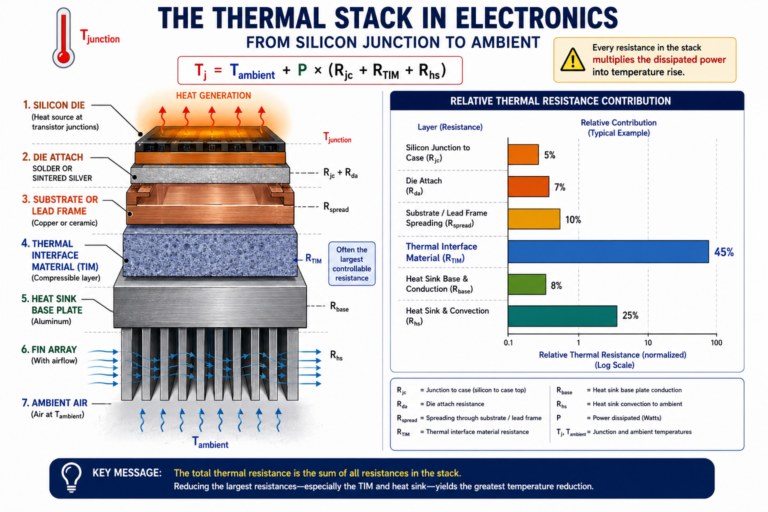
Thermal simulation allows engineers to predict temperature distributions in electronics assemblies before hardware is built, helping identify thermal risks, optimize cooling, and evaluate worst-case operating conditions.1
The power of the framework is that it decomposes the thermal problem into individual resistances that can be independently analyzed, optimized, and validated. Each resistance element has a physical identity (die attach, TIM, heat sink), a formula or datasheet source for its value, and a set of design variables that control it. Simulation’s role is to compute these resistances accurately for the actual three-dimensional geometry, something the 1D formula cannot do for complex geometries, and to identify which resistance elements dominate the total, guiding optimization effort toward the highest-leverage design changes.
| Resistance Element | Symbol | Formula / Source | Typical Value Range | What It Governs | How to Reduce It |
| Junction to case (die) | R_jc | Provided in component datasheet; governed by die size, bond wire layout, die attach material | 0.1–5.0 °C/W for ICs; 0.01–0.5 °C/W for power modules | Maximum power density the die can dissipate before junction temperature is exceeded | Larger die area; better die attach material (sintered silver vs solder); flip-chip vs wire bond |
| Die attach (solder/adhesive) | R_da | t/(k × A); t = thickness, k = thermal conductivity, A = area | 0.05–0.5 °C/W; sintered silver ~0.01 °C/W | Heat flow from die to substrate; first interface resistance below die | Reduce solder thickness; use sintered silver (k=200 W/mK) vs SAC solder (k=57 W/mK); maximize die attach area |
| Substrate / PCB spreading | R_spread | Depends on copper layer count, via density, board thickness | 0.5–5.0 °C/W for FR4 PCB; 0.1–1.0 °C/W for metal-core PCB (MCPCB) | Lateral heat spreading from component footprint to board area available for convection | Add copper pours; use thermal vias under component; switch to MCPCB or ceramic substrate for high-flux components |
| Thermal interface material (TIM) | R_TIM | t/(k × A); k = 0.5–80 W/mK depending on TIM type | 0.05–1.0 °C/W; phase-change TIM ~0.1 °C/W; thermal paste ~0.2 °C/W; dry contact ~1.0 °C/W | Interface between component case and heat sink, largest variable resistance in most systems | Use higher-k TIM; minimize bond line thickness (BLT); ensure surface flatness < 25 µm for paste/phase-change TIM |
| Heat sink (fin + base) | R_hs | 1/(h × A_fin); h = convection coeff, A_fin = fin area | 0.1–5.0 °C/W natural convection; 0.02–0.5 °C/W forced convection | Convection from heat sink to ambient air, governs total system thermal resistance floor | Increase fin area; reduce fin pitch for forced convection; use vapor chamber or heat pipe for spreading |
| Case to ambient (no heat sink) | R_ca | Complex, governed by board layout, enclosure, airflow | 2–20 °C/W for natural convection in enclosure | Total temperature rise from component case to ambient when no dedicated heat sink is used | Add local copper thermal pad; ensure airflow path; space high-power components for mutual air convection |
| PCB to ambient (conduction-cooled) | R_board | Depends on copper layer count and conduction path to chassis | 1–10 °C/W from component to chassis edge | Heat flow via PCB copper to chassis ground plane, dominant path in conduction-cooled military/space electronics | Maximize copper fill between component and chassis attachment; use copper-core PCB; minimize PCB-to-chassis thermal resistance |
When the 1D Model Fails: The Spreading Resistance Problem
The 1D thermal resistance model assumes heat flows in one direction, from the die straight down through the stack to the ambient. In reality, heat spreads laterally through every layer it passes through, expanding the effective heat transfer area as it moves away from the concentrated die heat source. This spreading increases the effective area for convection and reduces the thermal resistance below the 1D prediction, which sounds beneficial, but the spreading also creates lateral temperature gradients that the 1D model misses entirely
Spreading resistance (Rspread) depends on the heat-source area, spreading-layer area, layer thickness, and thermal conductivity. For a small 5 × 5 mm die on a large 150 × 100 mm PCB, a simple 1D model can underestimate the local temperature because it does not capture how heat spreads outward from the die.
A 2D or 3D thermal simulation captures this temperature gradient and shows whether the design is limited by poor heat spreading—requiring more copper or thermal vias—or by insufficient convection area, which may require a heat sink or increased airflow.
Thermal simulation software such as SimScale enables engineers to model heat transfer, temperature distribution, and cooling performance before physical prototypes are built.
The Effect of Adjacent Components: The Mutual Heating Problem
In a densely populated PCB, every high-power component raises the local ambient temperature for its neighbors. A component that dissipates 3W in isolation might operate at 55°C junction temperature. The same component placed 10mm from a 5W DSP, which raises the local air temperature by 15°C through its convective plume, operates at 70°C. This mutual heating effect is invisible to single-component thermal analysis and is one of the most common causes of field failures in products where each individual component was analyzed in isolation and found to be thermally safe.
System-level PCB thermal simulation, modeling the entire board with all components, their power dissipations, and the enclosure airflow, captures mutual heating automatically. The temperature at each component location includes contributions from all neighbors, not just the component’s own self-heating. The highest-risk components in a dense layout are not necessarily the highest-power ones, they are the ones with high thermal sensitivity (steep Arrhenius slope) placed in the thermal shadow of high-power neighbors. Identifying these components requires system-level simulation, not component-level analysis.
Thermal Simulation Fidelity Levels: Choosing the Right Tool
Electronics thermal simulation spans seven distinct fidelity levels, from a spreadsheet thermal resistance calculation to a full conjugate heat transfer CFD model with turbulent airflow, radiation, and thermal-structural coupling. Choosing the right fidelity level for each design decision is as important as building an accurate model, over-specifying the fidelity wastes time and compute resources on information that is not needed for the current design decision; under-specifying misses the physics that governs the outcome. The following table maps each method to its physics, accuracy, cost, and optimal use case.
| Tool / Method | Physics Captured | Accuracy Level | Computational Cost | Best For | Limitation |
| Thermal resistance network (1D/lumped) | Conduction only; 1D steady-state from junction to ambient via Rth chain | Order-of-magnitude; ±20–50% for complex geometries | Negligible, spreadsheet calculation | Early design, budgeting junction temperature, comparing cooling strategies at system level | Cannot predict spreading resistance, temperature gradients within PCB, or hotspot location |
| 2.5D PCB thermal analysis (layer-averaged) | Conduction through PCB layers; simplified convection boundary; copper spreading | Moderate, ±10–20% for temperature rise | Low, seconds to minutes | PCB layout thermal optimization; identifying hotspot components; copper pour placement | Misses 3D effects; cannot model component-level airflow; simplified convection not accurate in ducted or complex enclosures |
| 3D conduction FEA (no CFD) | Full 3D conduction; radiation (if included); boundary convection from convection coefficients | Good, ±5–15% with accurate convection coefficients | Medium, minutes to hours for detailed PCB model | Component-level thermal analysis; heat spreader design; TIM optimization; conduction-cooled board design | Convection coefficient is input, not computed, accuracy limited by quality of h values; cannot predict airflow-dependent cooling |
| Conjugate heat transfer CFD (3D coupled) | Full 3D conduction in solids + Navier-Stokes airflow; radiation optional; buoyancy for natural convection | High, ±3–10% for T_junction and flow patterns | High, hours to days for full system model | Enclosure thermal design; heat sink optimization; natural convection systems; blower/fan performance in complex geometries | High mesh count for simultaneous fluid and solid domains; long run time limits parametric exploration speed |
| Compact thermal model (JEDEC DELPHI) | Behavioural model representing IC package as network of resistances calibrated to detailed model | Good, matches detailed model within 5–10% across board conditions | Low, component is a simplified resistance network | System-level analysis with many components; board-level thermal map without modeling every component in detail | Must be calibrated from detailed model or datasheet; accuracy degrades outside calibration envelope |
| Transient thermal analysis (FEA/CFD) | Time-dependent conduction and convection; thermal mass (capacitance) of all elements | High for transient profiles; depends on material Cp accuracy | High, many time steps at full 3D model cost | Power cycling life prediction; junction temperature during pulsed loads; thermal runaway analysis; Tj-vs-time under startup | Thermal capacitance data (Cp, density) must be accurate; long run times for slow thermal systems (battery packs, enclosures) |
| Thermal-structural coupled (FEA) | Conduction FEA feeding temperature field into structural FEA; thermal stresses and warpage computed | Structural accuracy limited by thermal input accuracy; ±5–15% for stress if temperature is accurate | High, two coupled analyses | Solder joint fatigue prediction; PCB warpage; package CTE mismatch stress; connector retention under thermal cycling | Requires both accurate thermal model and accurate structural model; CTE mismatch data must be source-verified |
The Compact Thermal Model: Bridging Component and System Analysis
The JEDEC DELPHI compact thermal model standard provides a practical solution to the tension between component-level accuracy and system-level analysis efficiency. A JEDEC DELPHI model represents a complete IC package as a behavioural network of thermal resistances calibrated to match the detailed package thermal simulation across a range of board conditions, different copper areas, airflow rates, and power levels. The compact model captures the package’s thermal behaviour correctly without requiring the analyst to model every internal layer of the package explicitly.
The compact model’s input is the power dissipated by the component; its output is the junction temperature, given the board thermal conditions at the component’s attachment footprint. Because the model is computationally trivial (a small network of resistances), boards with 50 to 500 components can be analyzed in minutes using compact models for all components, a board-level analysis that would take days or weeks if every component were modeled in full 3D detail. The tradeoff: compact models are only accurate within their calibration envelope, and their accuracy degrades if the board conditions deviate significantly from the conditions under which they were calibrated.
The CFD Conjugate Heat Transfer Model: When Full Physics Is Required
Conjugate heat transfer (CHT) CFD simultaneously solves the Navier-Stokes equations for the fluid domain (airflow in the enclosure or heat sink) and the heat conduction equation for the solid domain (PCB, components, heat sink, enclosure), coupling them at all fluid-solid interfaces. The fluid temperature affects the solid temperature through convection; the solid temperature affects the fluid density and viscosity through buoyancy and property variation. CHT CFD is the only method that correctly computes the convection heat transfer coefficient h for complex enclosure geometries, the h that all lower-fidelity methods require as an input.
The applications where CHT CFD is necessary rather than optional: natural convection systems (where buoyancy-driven flow depends on the temperature field in a coupled manner that cannot be prescribed as a boundary condition), complex forced convection with multiple airflow paths and obstructions, fan operating point determination in a specific duct geometry, and any system where the thermal design is being optimized rather than validated. A heat sink fin pitch optimization without CHT CFD is not an optimization, it is a guess, because the convection coefficient and pressure drop change with fin pitch in ways that cannot be captured by a simple h boundary condition applied to a conduction-only model.
Thermally Activated Failure Mechanisms: What Simulation Must Predict
The value of thermal simulation in electronics is not temperature for its own sake, it is failure rate prediction. Every thermally activated failure mechanism has a quantitative relationship between temperature and failure rate, described by the Arrhenius equation: failure rate scales as exp(-E_a / kT), where E_a is the activation energy, k is Boltzmann’s constant, and T is the absolute temperature in Kelvin. The implication is direct: every 10°C reduction in junction temperature approximately halves the failure rate for mechanisms with activation energy around 0.7 eV, the most common range for semiconductor failure mechanisms. Conversely, every 10°C increase approximately doubles the failure rate.
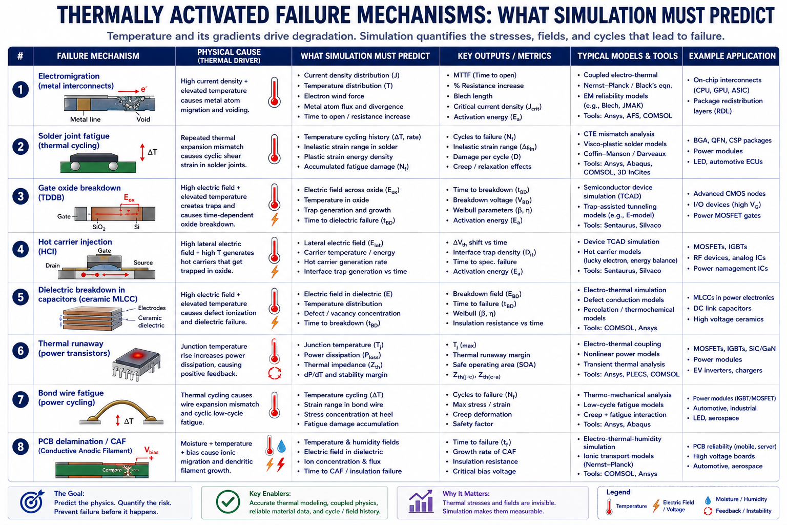
The failure rate relationship means that the thermal simulation’s accuracy requirement is set by the failure rate sensitivity, not by an absolute temperature accuracy. For a mechanism with 2x failure rate per 10°C, a 10°C error in junction temperature prediction doubles or halves the predicted failure rate, producing a reliability prediction that is off by a factor of 2 from the actual field failure rate. For safety-critical electronics (automotive, aerospace, medical) where the reliability target may be 1,000 to 10,000 FIT (failures per billion device hours), a factor-of-2 reliability prediction error is the difference between a compliant design and a field recall.
| Failure Mechanism | Temperature Dependence | Simulation Output Needed | Arrhenius Acceleration Factor (per 10°C) | Design Target |
| Electromigration (metal interconnects) | Exponential, activation energy 0.7–1.0 eV; doubles failure rate every 8–12°C | Peak metal layer temperature; current density distribution at via and metal necks | 2.0–2.8x per 10°C at operating range | Keep Tj < 85°C for standard ICs; < 105°C for automotive; via current density < 5×10^5 A/cm^2 |
| Solder joint fatigue (thermal cycling) | Coffin-Manson: N_f proportional to delta_T^{-alpha}; cycles to failure drop with temperature range | Temperature range delta_T per cycle; mean temperature Tm; plastic strain amplitude in solder | Cycle life halves for every 15–20°C increase in delta_T | Minimize delta_T per cycle; keep Tj < 100°C for SnAgCu solder on FR4; use underfill for fine-pitch BGA |
| Gate oxide breakdown (TDDB) | Strong temperature dependence, activation energy 0.7–1.1 eV; time-to-breakdown halves every 7–10°C above threshold | Gate oxide temperature, closely tracks junction temperature | 2.0–3.0x per 10°C | Keep Tj < datasheet maximum; typically 125°C for silicon CMOS; 150–175°C for automotive-grade |
| Hot carrier injection (HCI) | Worst at intermediate temperatures (25–75°C); less dominant at highest temperatures vs electromigration | Peak channel electric field; device current density; junction temperature | ~1.5–2.0x per 10°C for drain current stress | weakly temperature-dependent | Voltage derating at elevated temperature; transistor sizing to limit peak field |
| Dielectric breakdown in capacitors (ceramic MLCC) | Exponential, time to failure scales as exp(-E_a/kT); strong dependence above rated temperature | Capacitor body temperature; voltage stress | 2–4x per 10°C above rated temperature | Derate voltage to 50–80% of rated at operating temperature; keep temperature < 85°C or use 125°C rated parts |
| Thermal runaway (power transistors) | Positive feedback: higher T → lower R_ds(on) for BJT → more current → higher T | Dynamic junction temperature during switching; thermal impedance Z_th transient | Runaway threshold: depends on device and load line intersection | Ensure load line does not cross device’s safe operating area (SOA); use thermal protection circuit; verify Z_th(t) under pulse conditions |
| Bond wire fatigue (power cycling) | Thermal cycling between bond wire and die: CTE mismatch drives plastic deformation at heel of bond | Number of power cycles; peak and trough Tj per cycle; bond wire temperature gradient | Cycle life halves for every 10–15°C increase in delta_Tj per power cycle | Limit power cycle amplitude; use heavy aluminium or copper wire for power modules; use silver sintering instead of wire bond where possible |
| PCB delamination / CAF (Conductive Anodic Filament) | Accelerated by high temperature + high humidity; CAF growth rate exponential with temperature | PCB temperature map; identify copper features at risk of CAF between adjacent conductors | 3–5x per 10°C acceleration in highly accelerated life test (HALT/HAST) | Limit PCB temperature < 85°C for standard FR4; use halogen-free low-CTE laminates for high-reliability applications |
Electromigration: The Temperature-Current Density Interaction
Electromigration, the migration of metal atoms along grain boundaries under the force of electron momentum transfer, is the dominant long-term failure mechanism in semiconductor interconnects. The Black’s equation for electromigration mean time to failure is: MTF = A × J^{-n} × exp(E_a / kT), where J is the current density in the metal conductor, n is typically 1–2 for modern interconnects, and E_a is the activation energy (0.7–1.0 eV depending on the metal and interface).
Thermal simulation for electromigration must provide two outputs: the temperature at each metal layer (to evaluate the exp(E_a/kT) term) and the current density distribution (for the J^{-n} term). In practice, current density is computed by electrical simulation (IR drop analysis), and temperature is computed by thermal simulation with the current-density-dependent Joule heating as the heat source. The two simulations are coupled: current density generates heat, heat changes resistivity, changed resistivity changes current distribution. For high-current-density designs, an electrothermal co-simulation that couples the electrical and thermal solvers is required to correctly capture this interaction, a thermal-only simulation with fixed current density underestimates the temperature at high-current vias and metal necks.
Solder Joint Fatigue: Linking Thermal Cycling to Mechanical Failure
Solder joint fatigue is the most common thermally driven mechanical failure mode in electronic assemblies. The failure mechanism is thermal cycling: as the PCB temperature rises during operation and falls during standby, the differential thermal expansion between the component package (CTE ~6–15 ppm/°C depending on package type) and the PCB (CTE ~14–18 ppm/°C for FR4) drives plastic deformation in the solder joint. Each thermal cycle accumulates a small increment of plastic strain; after enough cycles, the accumulated damage initiates a fatigue crack that propagates to electrical open failure.
The Coffin-Manson relationship for solder fatigue is: N_f = C × (delta_epsilon_p)^{-alpha}, where N_f is the cycles to failure, delta_epsilon_p is the plastic strain range per cycle, and C and alpha are material constants (alpha ≈ 1.9 for SnAgCu lead-free solder). Thermal simulation provides the temperature range delta_T at the solder joint level; structural simulation converts this temperature range to plastic strain amplitude using CTE mismatch, package geometry, and solder constitutive behavior. Neither the thermal model alone nor the structural model alone can predict solder fatigue life, the coupled thermal-structural analysis is required, and accuracy demands that both the temperature field and the material plasticity model be correctly specified.
Heat Sink Design Optimization Through Simulation
Heat sink design is one of the most valuable applications of thermal simulation because the relationship between fin geometry and thermal performance is highly nonlinear. Simple analytical correlations can estimate the performance of an isolated fin array under uniform airflow, but they cannot fully capture real-world effects such as flow non-uniformity between fins, pressure drop and its impact on fan performance, heat spreading through the base, or thermal contact resistance at the component interface.
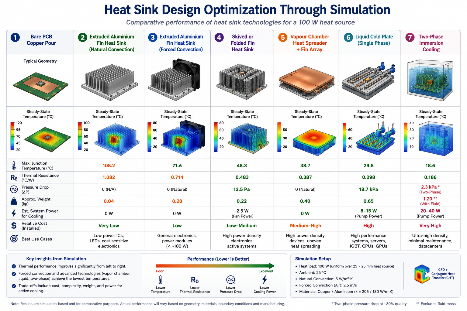
Conjugate heat transfer (CHT) CFD captures these effects together, allowing engineers to optimize the heat sink rather than simply select a standard catalog design. Fin pitch, height, thickness, and base thickness can be varied systematically to identify the geometry that provides the lowest thermal resistance for a specific fan, enclosure, power density, and airflow constraint.
| Heat Sink Type | Thermal Resistance Range | Airflow Requirement | Power Density (W/cm²) | Typical Application | Key Design Variable for Simulation |
| Bare PCB copper pour | 10–30 °C/W component-to-ambient | None (natural convection from copper surface) | < 0.1 W/cm² | Low-power ICs, microcontrollers, small regulators on consumer PCB | Copper pour size and shape; distance to board edge; copper layer count |
| Extruded aluminium fin heat sink (natural convection) | 2–10 °C/W | None, buoyancy-driven natural convection between fins | 0.1–0.5 W/cm² | Linear voltage regulators, small power supplies, industrial control modules | Fin height, pitch, thickness, base plate thickness, optimised by CFD natural convection sweep |
| Extruded aluminium fin heat sink (forced convection) | 0.2–2.0 °C/W | 0.5–5 m/s air velocity across fins | 0.5–5 W/cm² | Server CPUs, power amplifiers, motor drives, industrial electronics | Fin pitch optimisation for given fan curve; pressure drop vs flow rate; fan operating point intersection |
| Skived or folded fin heat sink | 0.05–0.5 °C/W forced convection | 2–10 m/s; dedicated blower or axial fan | 2–20 W/cm² | High-performance CPUs/GPUs, IGBT power modules, telecom base stations | Very thin fin pitch (0.5–1.5 mm) requires CFD for accurate pressure drop; fin-to-fin airflow uniformity |
| Vapour chamber heat spreader + fin array | 0.02–0.2 °C/W (spreading resistance near zero) | Any, separate from spreading function | 10–100 W/cm² on die; spreads to fin area | High-flux processors (>100W TDP), GPU packages, 5G mmWave power amplifiers | Effective spreading resistance vs die size; interface resistance at vapour chamber base; fin array optimisation above VC |
| Liquid cold plate (single phase) | 0.01–0.2 °C/W liquid-to-coolant | Coolant flow rate 1–10 L/min at 20–60°C inlet | 50–500 W/cm² | High-power server CPUs, IGBT stacks in EV inverters, data centre liquid cooling | Internal channel geometry (serpentine, pin-fin, micro-channel); pressure drop vs flow; coolant inlet/outlet temperature |
| Two-phase immersion cooling | 0.001–0.05 °C/W effective | Passive (pool boiling) or pumped two-phase | > 500 W/cm² peak; > 100 W/cm² sustainable | Extreme density data centres, HPC accelerator nodes, power electronics in electrified aviation | Boiling curve (heat flux vs superheat); nucleation site density; vapour bubble dynamics, requires specialised two-phase CFD |
Fin Pitch Optimization: Where CFD is Essential
The fin pitch optimization problem illustrates why CFD cannot be replaced by analytical formulas for heat sink design. Decreasing fin pitch increases the fin area per unit volume (good for heat transfer) but also increases the flow resistance through the fin channels (bad, reduces airflow for a given fan pressure). The optimal fin pitch is the one that maximizes heat transfer given the actual fan operating point, which itself depends on the fin array pressure drop.
The analytical approach: compute heat transfer coefficient h for a given pitch using the Dittus-Boelter correlation for turbulent channel flow; compute fin efficiency; compute thermal resistance. This approach misses: the entrance length effect (h is higher near the leading edge of each fin); the fin tip-to-shroud clearance effect (bypass flow reduces effective airflow through fins); the heat sink inlet flow non-uniformity; and the fan curve intersection with the system resistance curve. Each of these effects changes the optimum pitch by 10 to 30 percent.
CFD optimization workflow: parametrically vary fin pitch from 1.0mm to 4.0mm in 0.5mm steps, holding fin height, base thickness, and fan constant. For each pitch, the CHT CFD simulation computes: the actual airflow rate through the fin array (from the fan curve intersection with the computed system resistance), the local heat transfer coefficient distribution along each fin, the fin temperature distribution, and the junction temperature. The pitch that minimizes T_junction is the optimal design, and the result is typically 15 to 30 percent better thermally than the pitch selected by the analytical approach alone.
Vapour Chamber Integration: Simulation for Spreading-Limited Systems
When the die heat flux exceeds approximately 50 W/cm², the spreading resistance in a solid aluminium or copper heat sink base becomes the dominant thermal resistance, the fin array performance is irrelevant if the heat cannot spread from the die to the fin area fast enough. Vapour chambers, flat two-phase heat spreaders that use the evaporation-condensation cycle of a working fluid (typically water) to transport heat laterally with near-zero effective thermal resistance, address this limitation.
Thermal simulation of vapour chamber systems replaces the high spreading resistance of a conventional solid base with the much higher effective thermal conductivity of the vapour chamber. This effective conductivity is typically modeled at 5,000–50,000 W/mK, compared with about 200 W/mK for copper and 150 W/mK for aluminium.
The simulation applies this equivalent conductivity to the spreading layer, with conduction FEA or conjugate heat transfer (CHT) CFD used above and below it. The result is a more uniform base temperature and smaller temperature gradients across the heat sink. This also improves fin efficiency because the fins operate at more similar temperatures instead of the fins directly above the die running significantly hotter than those farther away.
Power Cycling and Transient Thermal Analysis
Steady-state thermal analysis answers the question: what is the junction temperature when the device has been operating at constant power long enough for the temperature to stabilize? Transient thermal analysis answers the question: what is the junction temperature at every moment in time during a time-varying power profile? For many electronics applications, the transient answer is more important than the steady-state answer, peak junction temperature may occur during a brief power spike that lasts milliseconds, not during sustained operation, and the failure mechanisms that respond to peak temperature (gate oxide breakdown, hot carrier injection, thermal runaway) are determined by the transient peak, not the steady-state average.
The Thermal Impedance Z_th: The Transient Thermal Resistance
The transient thermal behaviour of an electronic component is described by its thermal impedance Z_th(t), the ratio of junction temperature rise to applied power, as a function of time after a power step is applied. Unlike the steady-state thermal resistance R_th, which is a single number, Z_th(t) is a function that starts near zero (immediately after the power step, only the small thermal mass of the die itself has been heated) and rises asymptotically to R_th as the heat diffuses through all the thermal layers to the ambient.
The Z_th(t) curve is directly measurable from the die junction using the electrical test method (JEDEC JESD51-14) and is provided in power semiconductor datasheets as a standard parameter. For FEA thermal simulation, Z_th(t) is a primary validation target: a correctly built transient thermal model should match the measured Z_th(t) curve within 5 to 10 percent across the entire time range from 1 microsecond to steady state. Discrepancies at short time scales indicate incorrect material heat capacity (Cp × rho × volume) for the die or die attach; discrepancies at long time scales indicate incorrect thermal resistance in the package-to-board or board-to-ambient path.
Power Cycling Reliability: Simulation for Automotive and Industrial Applications
Power cycling, the repeated thermal cycling of a power semiconductor under electrical load, with junction temperature swings of 50 to 150°C per cycle, is the most accelerated degradation mechanism in power electronics. IGBTs in electric vehicle inverters may experience millions of power cycles over the vehicle lifetime, driven by the motor control current profile that generates hundreds of milliseconds-long current pulses at each motor commutation. Each current pulse heats the IGBT junction; each pulse off-time cools it. The repeated thermal strain accumulates fatigue damage in the bond wires and the solder die attach layers until one of them fails.
Transient thermal simulation for power cycling reliability requires: the junction temperature waveform T_j(t) for the actual drive cycle (current profile, ambient temperature, cooling conditions); the extraction of delta_T_j (the peak-to-trough junction temperature swing per power cycle); the mean junction temperature T_j_mean; and the number of cycles per hour of operation. These are fed into the power cycling lifetime model (typically a modified LESIT model or the Coffin-Manson-Arrhenius model from IEC 60747): N_f = A × (delta_T_j)^{-alpha} × exp(E_a / k T_j_mean). The simulation output directly predicts the number of power cycles to failure, which maps to vehicle lifetime in hours of operation given the drive cycle statistics.
Worked Example: Power Cycling Lifetime Calculation for EV Inverter IGBT |
Thermal-Structural Coupling: PCB Warpage and Solder Joint Stress
Thermal-structural coupling, using the temperature field from a thermal simulation as the input load to a structural FEA model, extends thermal simulation from temperature prediction to mechanical failure prediction. The two most important thermal-structural applications in electronics design are PCB warpage during reflow soldering (which determines whether components can be placed and soldered reliably) and solder joint fatigue under thermal cycling in service (which determines the product’s long-term reliability in the field).
PCB Warpage During Reflow: The Assembly Yield Problem
During reflow soldering, lead-free SAC assemblies typically reach peak temperatures of 230–260°C before cooling. Differences in thermal expansion between the PCB, components, and solder, combined with laminate relaxation at high temperatures, can cause permanent board warpage after cooling. Excessive warpage can lead to solder bridging, solder voiding, and head-in-pillow defects, particularly in large BGA packages.
Thermal-structural simulation of reflow warpage accounts for temperature-dependent material behavior, CTE mismatch between PCB layers and components, and the complete reflow temperature profile. The analysis predicts warpage throughout the heating and cooling cycle and after the board returns to room temperature. Engineers can then adjust the PCB stackup, copper distribution, or stiffening features before production, reducing assembly defects and improving manufacturing yield.
Solder Joint Stress Under Thermal Cycling: Field Life Prediction
For products that will experience thermal cycling in service, automotive electronics between -40°C and 125°C, outdoor telecom equipment between -40°C and 85°C, consumer electronics in daily use between 15°C and 85°C, solder joint fatigue life prediction through thermal-structural simulation is the primary reliability design tool. The simulation provides what no accelerated test can provide: a physics-based prediction of solder joint life at the actual field thermal cycle profile, mapped to an equivalent number of field cycles from the accelerated test conditions.
The thermal-structural workflow for solder joint reliability involves four steps: (1) simulate the thermal cycle to determine the temperature history at each solder joint; (2) use temperature-dependent SAC solder properties to calculate plastic strain accumulation during each cycle; (3) apply a Coffin-Manson fatigue model to estimate cycles to failure; and (4) compare the predicted fatigue life with the expected number of thermal cycles over the product’s design life.
The most critical solder joints are typically located at the corners of large BGA, QFP, and LGA packages. These joints have the greatest distance from the package center, known as the distance to neutral point (DNP). Because CTE mismatch displacement increases with DNP, corner joints generally experience the highest cyclic strain and fatigue risk.
Battery and EV Power Electronics: The Emerging Frontier
The electrification of transportation has created two new high-priority applications for thermal simulation in electronics: battery pack thermal management and high-voltage power electronics cooling for inverters, DC-DC converters, and on-board chargers. Both applications involve higher power densities, higher voltages, and more demanding duty cycles than traditional electronics, and both have failure modes (thermal runaway in batteries, bond wire fatigue in inverter IGBTs) where thermal simulation directly prevents catastrophic failures.
Battery Pack Thermal Simulation: Preventing Thermal Runaway
Thermal runaway, the uncontrolled self-heating of a lithium-ion battery cell that leads to electrolyte vaporization, separator failure, and potentially fire, is the catastrophic failure mode that battery thermal management simulation is specifically designed to prevent. The simulation challenge is that thermal runaway is a nonlinear positive feedback event: heat generation from the electrochemical reactions in the cell increases exponentially with temperature, and if the heat generation exceeds the heat removal capacity of the thermal management system, the temperature rises until the cell vents and ignites.
Battery thermal simulation supports thermal runaway prevention through three key analysis types: steady-state thermal analysis for normal operation, transient thermal analysis for fast charging and peak discharge, and thermal propagation analysis for single-cell runaway scenarios. These analyses help verify cell temperatures, predict temperature rise during high-power operation, and determine how effectively the thermal management system limits heat propagation to neighboring cells.
Thermal propagation analysis is particularly important for EV battery safety, where regulations such as UN ECE R100 and GB/T 38661 address thermal safety and propagation risks. Simulation helps engineers evaluate these scenarios early, identify thermal management weaknesses, and improve battery pack safety before physical testing.
SiC and GaN Power Electronics: Higher Temperature, Higher Frequency
Silicon carbide (SiC) and gallium nitride (GaN) power semiconductors are increasingly replacing silicon IGBTs in high-efficiency power electronics. Their ability to switch at higher frequencies with lower switching losses enables smaller passive components and higher power density. However, their higher power density also creates new thermal-management challenges. SiC MOSFETs can operate at junction temperatures up to 175°C, while some GaN devices can reach 200°C, creating high local heat fluxes in compact packages.
Thermal simulation for SiC and GaN systems must account for temperature-dependent material properties across a wider temperature range than traditional silicon-based designs. The power loop’s parasitic inductance also affects switching speed and losses, creating stronger coupling between electrical and thermal behavior. For high-fidelity analysis, electrothermal co-simulation simultaneously solves the circuit and thermal equations, capturing how switching losses affect temperature and how temperature, in turn, changes device performance.
The Electronics Thermal Simulation Workflow: From Schematic to Reliability Prediction
The complete thermal simulation workflow in electronics design follows a defined sequence of increasing fidelity, with decision gates at each stage that determine whether to proceed, iterate, or escalate to a higher-fidelity model. This workflow maps directly to the design stage, the fidelity of the thermal analysis should match the maturity of the design, with simple models at early concept stages and full CHT CFD and thermal-structural analysis at the detailed design stage before manufacturing release.
- Schematic / concept stage, 1D thermal resistance network: Compute T_junction for each high-power component using the datasheet R_jc, estimated board R_ca, and the cooling system R_hs. Identify components within 20°C of their maximum rated junction temperature. Flag these for closer attention in subsequent stages. This analysis takes hours and can be done in a spreadsheet before any PCB layout exists.
- PCB layout stage, 2.5D board-level thermal map: Import the PCB layout and component power dissipations. Run a 2.5D thermal analysis to generate the board temperature map. Identify hotspot locations and the components in the thermal shadow of high-power neighbors. Optimize copper pour placement, component spacing, and thermal via pattern based on the temperature map. This iteration loop runs in minutes per variant and can be completed within the PCB layout process.
- Detailed design stage, 3D conjugate heat transfer CFD: Build the full 3D enclosure model with fan or blower, PCB with all significant components, and detailed heat sink geometry. Run CHT CFD to determine the actual airflow distribution, the fan operating point in the system, the temperature distribution throughout the enclosure, and the junction temperatures of all critical components. Use this model to finalize heat sink geometry, fan selection, and component placement before tooling release.
- Reliability verification, thermal-structural coupled analysis: For the finalized design, run the coupled thermal-structural analysis to predict solder joint fatigue life under the field thermal cycle profile. Run transient analysis with the power profile to predict Z_th(t) correlation and peak junction temperature under pulsed loads. Verify that the design meets all thermal reliability targets before first article prototype builds.
- Prototype correlation, simulation update: Instrument the prototype with thermocouples or infrared measurement at key locations. Compare measured temperatures against simulation predictions. Update the simulation model to match measurements, typically by adjusting TIM thermal resistance and convection coefficients. The updated model becomes the validated model for design variant analysis and for extrapolating to environmental conditions not tested in the prototype phase.
| CRITICAL: Thermal Simulation Must Use Worst-Case Conditions, Not Typical One of the most common mistakes in electronics thermal simulation is analyzing only nominal conditions, typical power, 25°C ambient temperature, sea-level pressure, and unrestricted airflow. A design that passes under these conditions may still fail in the field when maximum power, high ambient temperature, altitude, and restricted airflow occur together. For reliable thermal design, simulations should evaluate worst-case operating conditions, including maximum power, maximum ambient temperature, reduced air density at altitude, and potential airflow restrictions such as clogged filters or blocked intakes. Nominal-condition analysis is useful for understanding normal operation, but worst-case thermal analysis is essential for establishing thermal compliance and reliability. |
Frequently Asked Questions
Q: What is junction temperature and why is it the primary output of electronics thermal simulation?
Junction temperature (Tj) is the temperature at the active semiconductor junction where switching and current conduction occur. It is the key output of electronics thermal simulation because semiconductor reliability models and datasheet temperature limits are based on Tj.
Case or package temperature is lower than Tj because heat flows through the junction-to-case thermal resistance. For example, a device with a 60°C case temperature can still have a 125°C junction temperature if power dissipation creates a 65°C temperature difference. Accurate Tj prediction therefore requires thermal simulation or direct thermal measurement.
Q: How accurate does thermal simulation need to be for electronics reliability prediction?
The required thermal simulation accuracy depends on the failure mechanism and how close the device operates to its junction-temperature limit. For electromigration and other Arrhenius-based mechanisms, a ±5°C error can produce about a 1.4× error in failure-rate prediction, while a ±10°C error can produce roughly a 2× error, which may be unacceptable for safety-critical applications.
For solder joint fatigue, accuracy in the temperature range (ΔT) per cycle is more important. A ±5°C error in ΔT can change predicted fatigue life by approximately 25%. In practice, validated CHT CFD models can achieve ±3–8°C junction-temperature accuracy compared with thermocouple measurements. However, uncertainty in input power and ambient-temperature distribution can often have a greater impact than simulation accuracy itself.
Q: What is a thermal via and how does simulation determine how many are needed?
A thermal via is a plated through-hole designed to transfer heat from a component’s top copper layer through the low-conductivity FR4 laminate to inner or bottom copper layers. PCB thermal simulation can optimize the via count and pattern by evaluating spreading resistance based on via diameter, spacing, fill material, and geometry.
For example, a 4×4 array of 0.3 mm solder-filled vias at 0.6 mm pitch under a QFN package can reduce PCB spreading resistance by 40–60% compared with no thermal vias. For a 2 W device on standard FR4, this can reduce junction temperature by approximately 8–15°C.
Q: What is the difference between thermal resistance and thermal impedance?
Thermal resistance (Rth) is a steady-state measure of temperature rise per unit of power dissipation once the system reaches thermal equilibrium. Thermal impedance (Zth) is a transient measure that describes how temperature rises after a power step is applied. Zth starts near zero and gradually approaches Rth as heat spreads through the device and surrounding materials.
This distinction is important for pulsed-power applications. For example, a device with an Rjc of 1.0°C/W may have a Zth of only 0.05°C/W at 1 ms, allowing much higher short-duration power without exceeding the maximum junction temperature. Thermal simulation should therefore account for both steady-state thermal resistance and transient thermal impedance.
Q: Can I use a thermal simulation to replace thermal testing of prototypes?
Thermal simulation should complement prototype testing, not replace it. Its purpose is to identify and resolve most thermal problems before the first prototype is built, turning prototype testing into a validation exercise rather than a problem-discovery exercise.
Once the simulation is correlated with thermocouple or infrared measurements, the validated model can be used to evaluate design variants, operating conditions, and environmental scenarios that were not physically tested. The ideal workflow is simulate → prototype → validate → optimize. Simulation reduces interim test iterations, while physical testing remains essential for final qualification where required by standards such as AEC-Q and MIL-STD-810.
Q: What material properties are most critical for accurate electronics thermal simulation?
The material properties with the greatest impact on thermal simulation accuracy are:
- TIM thermal conductivity (kTIM): The thermal interface material between the component and heat sink can be a major source of thermal resistance. Its conductivity ranges from about 0.5–80 W/m·K, depending on the material.
- PCB through-plane conductivity (kz): FR4 typically has a low kz of about 0.3 W/m·K. Copper via fill can significantly improve heat transfer to inner layers, so the correct effective conductivity is important.
- Die-attach conductivity: Standard SAC solder has a conductivity of about 57 W/m·K, while sintered silver can reach approximately 200 W/m·K. Using incorrect values can distort the predicted thermal resistance below the die.
- Heat capacity (Cp × ρ): This is critical for transient analysis because it determines the thermal time constant and affects the predicted thermal impedance Zth(t).
For reliable results, use material properties from supplier datasheets or certified databases rather than generic textbook values.
Conclusion:
The thermal failure mechanisms that govern electronics reliability, including electromigration, solder joint fatigue, gate oxide breakdown, and bond wire failure, are highly sensitive to temperature. Even a small error in junction temperature can significantly affect predicted failure rates. For products with demanding reliability targets, accurate thermal prediction is therefore a critical part of the design process.
Thermal simulation provides engineers with a way to predict junction temperatures before prototypes exist and across a wide range of operating conditions. While a 1D thermal resistance model is useful for early estimates, it may miss mutual heating between components, PCB temperature gradients, airflow variations, and transient temperature peaks. These effects can shift junction temperature enough to produce non-conservative reliability predictions.
The seven thermal simulation fidelity levels discussed in this article provide a practical path from early design screening to detailed validation. Simple thermal resistance models are useful for initial decisions, while CHT CFD, transient thermal analysis, and thermal-structural simulation provide greater detail when the design requires it. Used progressively and validated against physical testing, thermal simulation helps engineers identify thermal risks earlier, reduce prototype iterations, and build greater confidence in electronics reliability before production.
Deepen your simulation knowledge with our guides on CFD vs wind tunnel testing, why simulation fails, FEA preprocessing, static vs dynamic analysis, and how leading industries deploy simulation to prevent failures and reduce development cost.


Leave a Reply